
Description
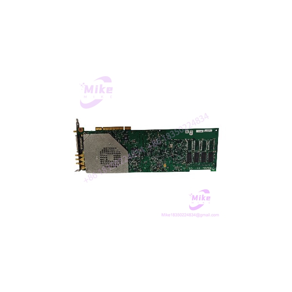
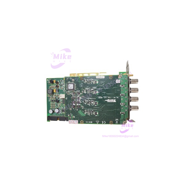
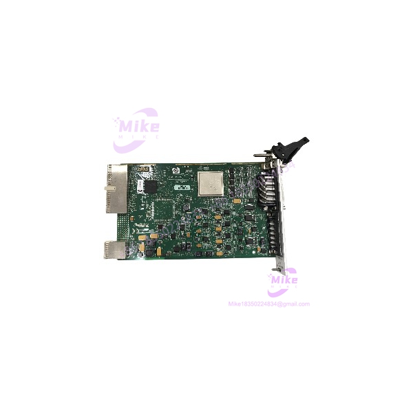
NI PXI-7852R | 8 AI 8 AO 96 DIO R-Series DAQ Card
Dynamic Product Introduction
Field engineers maintaining high-speed hardware-in-the-loop (HIL) simulators or custom digital protocol test stands know how demanding user-defined FPGA execution can be. When legacy test benches lose processing throughput or timing synchronization, replacing the hardware core without rewriting LabVIEW FPGA code is crucial.
The NI PXI-7852R features a dedicated Xilinx Virtex-5 LX50 FPGA alongside independent analog-to-digital converters (ADCs) on every analog input channel. Unlike multiplexed DAQ cards that share single converters across ports, the PXI-7852R provides true simultaneous sampling up to 750 kS/s per channel across all 8 analog inputs, combined with 8 simultaneous analog outputs updating at 1 MS/s. Paired with 96 high-speed digital lines capable of custom timing up to 80 MHz, the PXI-7852R provides the deterministic hardware execution required for aerospace simulation, power electronics control, and rapid prototyping.
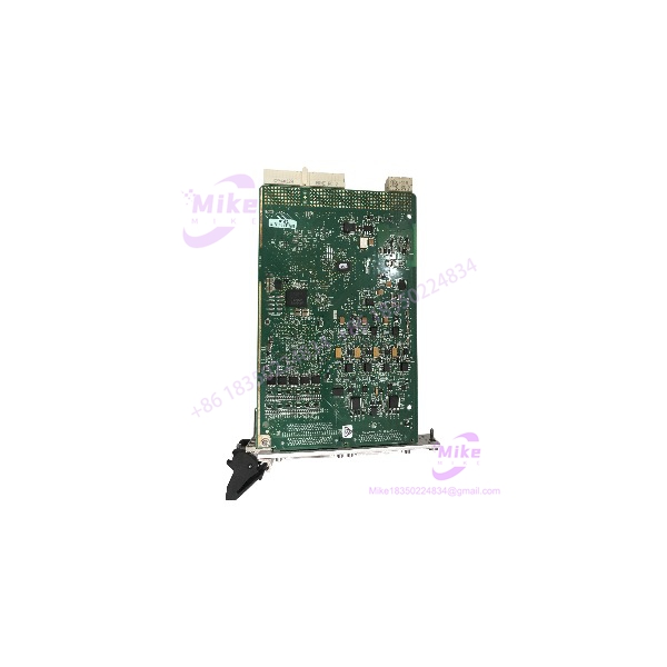
PXI-7852R
Key Technical Specifications
- FPGA Architecture: Xilinx Virtex-5 LX50
- Analog Input Channels: 8 differential channels (dedicated ADC per channel)
- AI Resolution & Rate: 16-bit, 750 kS/s simultaneous sampling per channel
- AI Input Range: Software-selectable ±1 V, ±2 V, ±5 V, ±10 V
- Analog Output Channels: 8 channels (dedicated DAC per channel)
- AO Resolution & Rate: 16-bit, 1 MS/s simultaneous update per channel
- AO Output Range: ±10 V
- Digital I/O Lines: 96 bidirectional TTL/CMOS lines (divided into 4 24-bit connectors)
- Maximum DIO Clock Rate: Up to 80 MHz
- Onboard Memory: Direct DMA channels to PXI host system (up to 16 DMA channels)
- Bus Interface: 32-bit PXI / CompactPCI slot interface
- Connector Type: 4 female 68-pin high-density SCSI connectors
Global Sourcing & Live-Test SOP (Transparency Core)
Sourcing legacy FPGA-based hardware requires comprehensive testing to ensure the onboard logic cells and dedicated converters operate without signal degradation.
Inbound Verification & Traceability
- Paperwork Audit: Validation of serial numbers against OEM manufacturing records to guarantee board authenticity and revision tracking.
- Physical Inspection: Detailed examination of all four 68-pin SCSI connectors, PCI edge contacts, PCB ground planes, and thermal pads on the Virtex-5 FPGA.
Live Rack Simulation & Diagnostics
- PXI Backplane Verification: Board is loaded into a PXI test chassis running PXI Trigger Bus lines to verify PCI recognition, DMA buffer allocation, and host communications.
- FPGA Bitfile Flashing & Execution: Compiling and flashing custom LabVIEW FPGA test routines to evaluate 100% of the Virtex-5 LX50 logic slices, block RAM, and DSP multipliers.
- Simultaneous I/O Testing: Driving all 8 AI channels and 8 AO channels simultaneously at maximum sampling rates (750 kS/s AI / 1 MS/s AO) while checking signal integrity and signal-to-noise ratio on a digital oscilloscope.
- 24-Hour Stress Run: Module undergoes a continuous 24-hour burn-in under maximum FPGA logic power draw inside a thermal chamber to verify zero thermal drift or dropouts.
Final Prep
- Flash Memory Verification: Verifying onboard non-volatile flash memory for default bitfile loading routines.
- ESD Safe Handling: Module is sealed in anti-static shielding bags with moisture absorbers before shipment.
The Field Engineer’s Pitfall Guide
- ❗ LabVIEW FPGA Module Version Dependencies: When replacing a PXI-7852R, verify that your host system’s LabVIEW FPGA Module and NI-RIO driver version support the exact FPGA target. Upgrading software environments without updating driver support targets can cause bitfile compilation failures or runtime device communication timeouts.
- ❗ DMA Channel Allocation Limits: The card supports up to 16 concurrent DMA FIFO channels. If your legacy host code attempts to open more DMA streams than configured in the target bitfile, the host system will throw an unhandled hardware memory exception on initialization.
- ❗ Digital I/O Drive Current & Grounding: The 96 digital lines are connected directly to FPGA I/O buffers. Exceeding current ratings per line (over 4 mA per pin) or leaving floating signal grounds on long external cable runs can permanently damage individual FPGA pin banks. Always ensure proper signal termination and common grounding.
Intent-Driven FAQ
Will replacing a damaged PXI-7852R wipe my custom FPGA bitfile?
No. Your custom FPGA bitfile is compiled and stored within your host software application on the controller PC. Upon initial application startup, the host system downloads the compiled bitfile to the FPGA RAM on the PXI-7852R, or you can configure it to flash non-volatile onboard memory.
Can I run the PXI-7852R in a PXI Express (PXIe) chassis?
The PXI-7852R uses a standard 32-bit PXI/CompactPCI connector. It can be installed in standard PXI slots or hybrid PXIe slots, but it will not physically fit or function in dedicated PXIe-only slots.
How does simultaneous sampling on the PXI-7852R differ from standard multiplexed DAQ cards?
Standard DAQ cards share a single analog-to-digital converter (ADC) across multiple channels via a multiplexer, which introduces phase delays between channels. The PXI-7852R features a dedicated 16-bit ADC on every single analog input channel, allowing true simultaneous phase-aligned sampling at 750 kS/s per channel.
What cables are required to break out the 96 digital I/O lines?
The card uses four 68-pin female high-density SCSI connectors (Connector 0 through Connector 3). NI recommends using shielded SH68-68-EPR cables paired with SCB-68 or CB-68LP connector blocks for isolated wiring.
What warranty is provided with replacement modules?
Verified PXI-7852R hardware sourced through qualified procurement channels includes a 12-month full replacement or repair warranty covering component performance and system stability.