


Description
Lam Research 810-234640-312 | RF Generator Interface PCBA Core Category
Dynamic Product Introduction
Chamber striking failures and plasma instability on older dielectric etchers usually point back to a degrading control node in the power delivery loop. When high-frequency tuning feedback loops drift, wafer yield drops instantly due to impedance mismatches. The Lam Research 810-234640-312 printed circuit board assembly intercepts these transients, delivering the deterministic signal processing required to keep plasma density locked.
Unlike generic automation input-output cards, this module manages sensitive RF analog feedback paths with specialized optical isolation to block ground loops—a common culprit behind intermittent tool alarms. Maintaining tight etch profiles on legacy platforms depends entirely on clean signal handshakes here, making this assembly a critical spare for fab floor uptime.
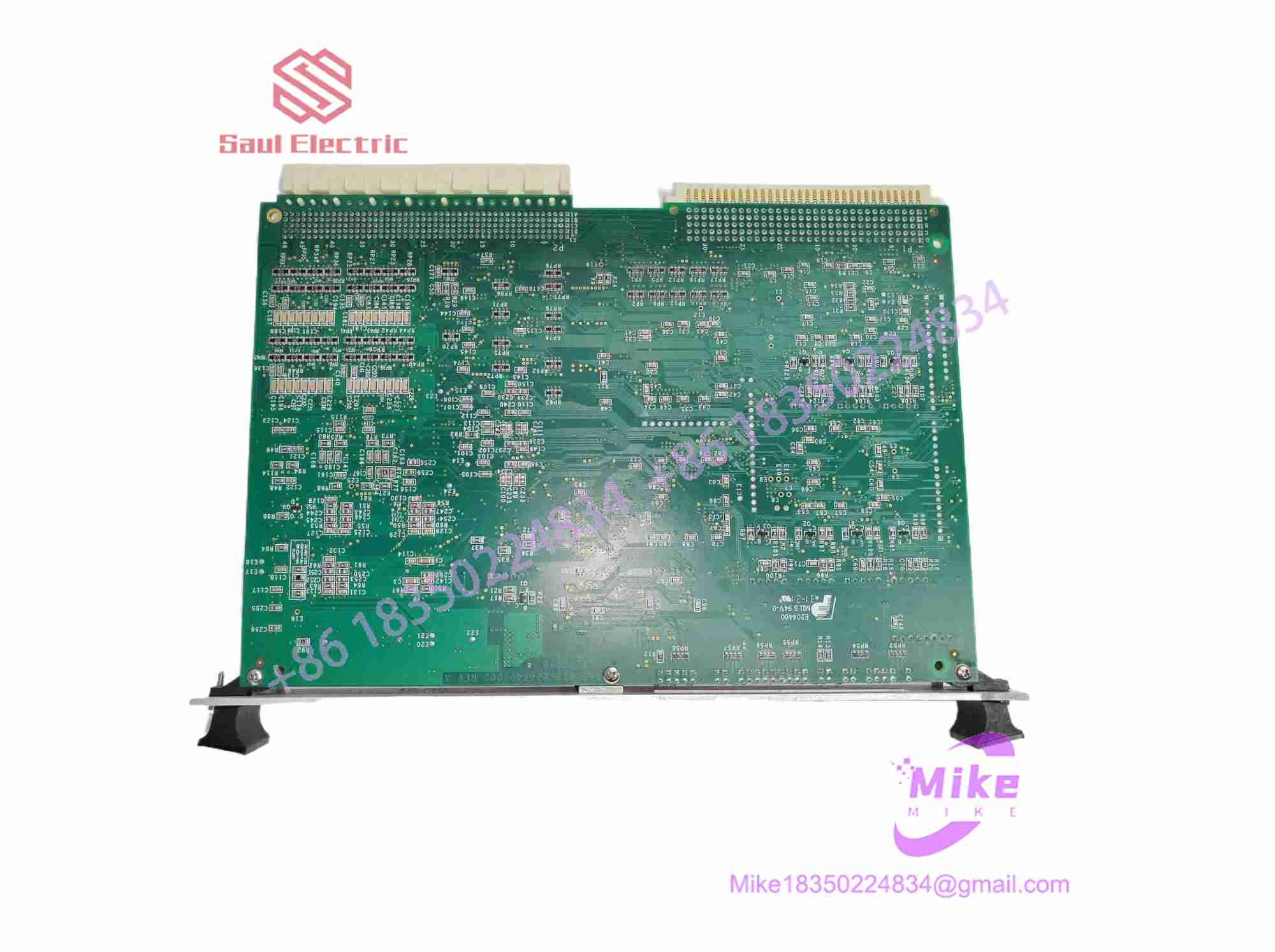
810-234640-312
Key Technical Specifications
| Parameter | Specification Detail |
| Manufacturer | Lam Research |
| Assembly Part Number | 810-234640-312 |
| Primary Architecture | RF Power Interlock and Tuning Control Board |
| Isolation Type | High-Voltage Optical Isolation on Critical I/O |
| Form Factor | Proprietary Slot-Mount Card Cage PCBA |
| Signal Conversion | High-Speed Analog-to-Digital / Digital-to-Analog Subsystem |
| Interlock Response Time | Sub-millisecond hardware safety trip loops |
| Diagnostic Interface | On-board status LEDs and test point arrays |
| Operating Environment | Cleanroom tool chassis (15^\circ C to 30^\circ C, non-condensing) |
Global Sourcing & Live-Test SOP (Transparency Core)
Handling high-frequency control electronics demands rigorous testing standards to ensure zero drift or latent component fatigue before the board touches a live chassis. Our multi-stage protocol guarantees field readiness:
- Inbound Verification: Incoming assemblies undergo microscopic trace inspection to check for solder micro-cracks or heat stress near high-dissipation power regulators. Original OEM serialization and revision levels are authenticated against global traceability logs.
- Live Simulation: We slide the PCBA into a dedicated diagnostic test bench configured to simulate real-world chamber load variations and high-frequency interference.
- Diagnostics: Technicians execute full-scale analog sweeps across all channels, measuring signal attenuation and verifying optical isolation integrity with precision oscilloscopes. Interlock trip times are verified down to the microsecond using synchronized timing generators, followed by an accelerated 24-hour thermal soak cycle.
- Final Prep: Post-test firmware registers and calibration offsets are documented. The board is then packed in heavy-duty ESD dissipative foam and hermetically heat-sealed inside a moisture-barrier bag.
The Field Engineer’s Pitfall Guide
❗ Ignoring Ground Plane Continuity: Failing to secure the board’s mounting thumbscrews tightly can lift the high-frequency ground plane reference, injecting severe noise into the RF matching network feedback loops and causing random tool aborts.
❗ Firmware Revision Mismatches: Dropping this module into a rack running an older system software version without checking firmware compatibility can result in communication timeouts with the master controller—freezing recipe execution mid-etch.
❗ Neglecting Calibration Trims: I’ve seen techs swap power interface boards and immediately run production without verifying analog zero-offsets, leading to immediate plasma ignition overshoots that burned up focus rings. Always verify calibration values against the equipment logs before clearing the tool for use.
Intent-Driven FAQ
Can I install the 810-234640-312 board while the tool electronics rack is powered on?
Never. This assembly handles sensitive analog control lines and high-voltage safety interlocks. Hot-plugging risks voltage spikes that can permanently damage the onboard conversion ICs and trip hard system safety faults.
Are calibration settings retained on the module or stored in the central host?
Core hardware configurations and baseline communication settings reside locally on the board’s onboard memory, while recipe-specific tuning parameters remain managed by the master tool computer. Always verify offset values after a swap.
What kind of warranty comes with this refurbished circuit board?
We provide a full one-year replacement warranty covering any functional or material defects under normal fab operating conditions.
How do I test if my RF tuning issue is caused by this board or the matching network itself?
Inspect the diagnostic LED array on the front edge of the PCBA. If the communication heartbeat is steady but analog feedback values fluctuate wildly during a match sweep, use an oscilloscope at the designated test points to isolate whether the signal degrades before or after the conversion stage.